Research Output
A showcase of the group’s representative publications, research projects, patents, and related academic achievements.
Representative Publications
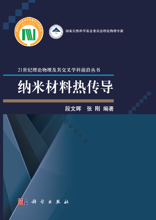
- [1] Wenhui Duan and Gang Zhang, Thermal Transport in Nanomaterials, Science Press, 2017.
- [2] Gang Zhang and Wenhui Duan, “Novel Physical Effects in Thermal Transport of Nanomaterials,” Physics, 49(10), 668–678 (2020).
- [3] “Size-Dependent Phononic Thermal Transport in Low-dimensional Nanomaterials,” Physics Reports, 860, 1–26 (2020).
- [4] “Anomalous strain effect on the thermal conductivity of low-buckled two-dimensional silicene,” National Science Review, 8(9), nwaa220.
- [5] “Phononic Weyl pair, phononic Weyl complex, phononic real Chern insulator state, and phononic corner modes in 2D Kekulé-order graphene,” Applied Physics Reviews, 10, 031416 (2023).
2. Dynamically Reversible Thermal Regulation under Multiphysics Coupling
Reversible dynamic thermal regulation has broad application prospects in integrated-circuit thermal management, the new energy industry, aerospace, and related fields. The group has systematically investigated the mechanisms and performance of thermal switches based on a wide range of solid materials, including ferroelectric materials, ferromagnetic materials, nanomaterials and nanostructures, polymers, and phase-change materials. Multiple control strategies and potential mechanisms for enhancing thermal-switch performance have also been explored.
- [1] “Actively and reversibly controlling thermal conductivity in solid materials,” Physics Reports, 1058, 1–32 (2024).
- [2] “Spin-gapless semiconductors for future spintronics and electronics,” Physics Reports, 888, 1–57 (2020).
- [3] “Giant Thermal Switching in Ferromagnetic VSe2 with Programmable Switching Temperature,” Nanoscale Horizons, 8, 202–210 (2023).
- [4] “Manipulating interfacial thermal conduction of 2D Janus heterostructure via a thermo-mechanical coupling,” Advanced Functional Materials, 32(18), 2110846 (2022).
- [5] “Thermo-mechanical correlation in two-dimensional materials,” Nanoscale, 13, 1425 (2021).
3. Artificial Intelligence-Accelerated Materials Design and Development
Thermoelectric materials provide important solid-state solutions for waste-heat recovery and cooling. Over the past decades, improving thermoelectric performance has remained a central challenge in the field, typically requiring the coordinated optimization of multiple interrelated physical parameters. In recent years, the group has introduced artificial intelligence into thermoelectric materials research and improved thermoelectric conversion efficiency through the optimization of key physical parameters across multiple material systems.
In 2022, the group initiated and hosted the International Conference on Intelligent Materials Design, centered on the application of artificial intelligence and deep learning to the prediction of new materials and material properties. Three editions of the conference series have been successfully held to date, bringing together hundreds of experts and scholars from China and abroad and continuously promoting international academic exchange and collaboration in this frontier interdisciplinary field.
- [1] “Machine Learning Approaches for Thermoelectric Materials Research,” Advanced Functional Materials, 30, 1906041 (2020).
- [2] “Material Platforms for Defect Qubits and Single Photon Emitters,” Applied Physics Reviews, 7, 031308 (2020).
- [3] Artificial Intelligence for Materials Science, Tian Wang, Yuan Cheng, Gang Zhang, Springer, 2021.
Patents and Intellectual Property
- [1] Preparation Method of Surface-State Nano Silver Oxide for Low-Temperature Solid-State Interconnection Technology, ZL 2022 1 0806826.1 (Invention Patent)
- [2] Interconnection Method and Interconnection Structure of Copper/Silver-Based Solid-Solution Composite Bumps, ZL 2024 1 1188988.9 (Invention Patent)
- [3] Micro-Interconnection System Based on an Ultrasonic-Laser Coupling Mechanism, ZL 2024 1 1536676.2 (Invention Patent)
Highlights
Technical Field Advanced MaterialsSilicon Nitride Ceramic AMB Copper-Clad Substrates
Owing to their high reliability, high thermal conductivity, excellent mechanical performance, and favorable coefficient-of-thermal-expansion matching, silicon nitride active metal brazed (AMB) substrates have become critical packaging substrates for high-temperature power semiconductor devices. They play a central role in the packaging of insulated-gate bipolar transistor (IGBT) power control modules, high-power light-emitting diodes (LEDs), high-power lasers, and related devices.
Compared with direct bonded copper (DBC) substrates, silicon nitride AMB substrates exhibit significant advantages in thermal conductivity, current-carrying capability, and thermal-expansion compatibility, thereby substantially improving the reliability of high-power devices. At present, silicon nitride AMB substrates are gradually replacing alumina- or aluminum-nitride-based DBC substrates and are emerging as a major development direction in high-power electronic packaging, where they serve as a key factor governing overall performance, reliability, and service lifetime.
The high-thermal-conductivity, high-toughness silicon nitride ceramic substrates developed by the group have reached an internationally advanced level in key technical parameters, with thermal conductivity stably exceeding 85 W/m·K and average flexural strength surpassing 800 MPa. In collaboration with leading industrial partners, future production capacity is expected to expand further, positioning the team as a major domestic supplier of silicon nitride ceramic substrates and enabling progressive convergence with the international state of the art. This will support the independently controllable mass production of silicon nitride ceramic substrates featuring high precision, high thermal conductivity, low thermal resistance, exceptional reliability, and long-term durability.
In parallel, the coordinated development of active-metal brazing copper-cladding processes and related packaging test technologies supports the independent research, development, and production of the entire chain of key materials, key processes, and key equipment, thereby contributing to the continued advancement of integrated-circuit packaging and high-power device modules in China.
Project Images
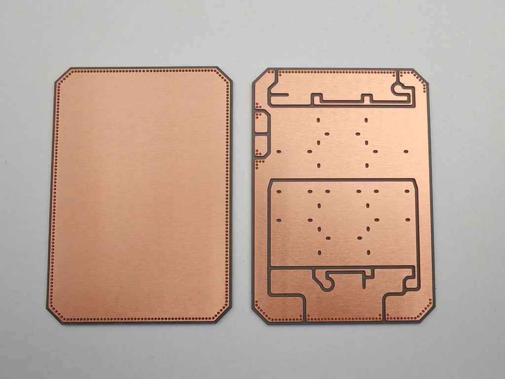
AMB Silicon Nitride Ceramic Copper-Clad Substrate
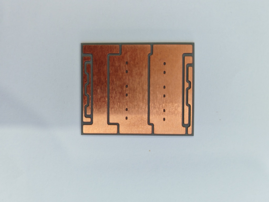
AMB Silicon Nitride Ceramic Copper-Clad Substrate
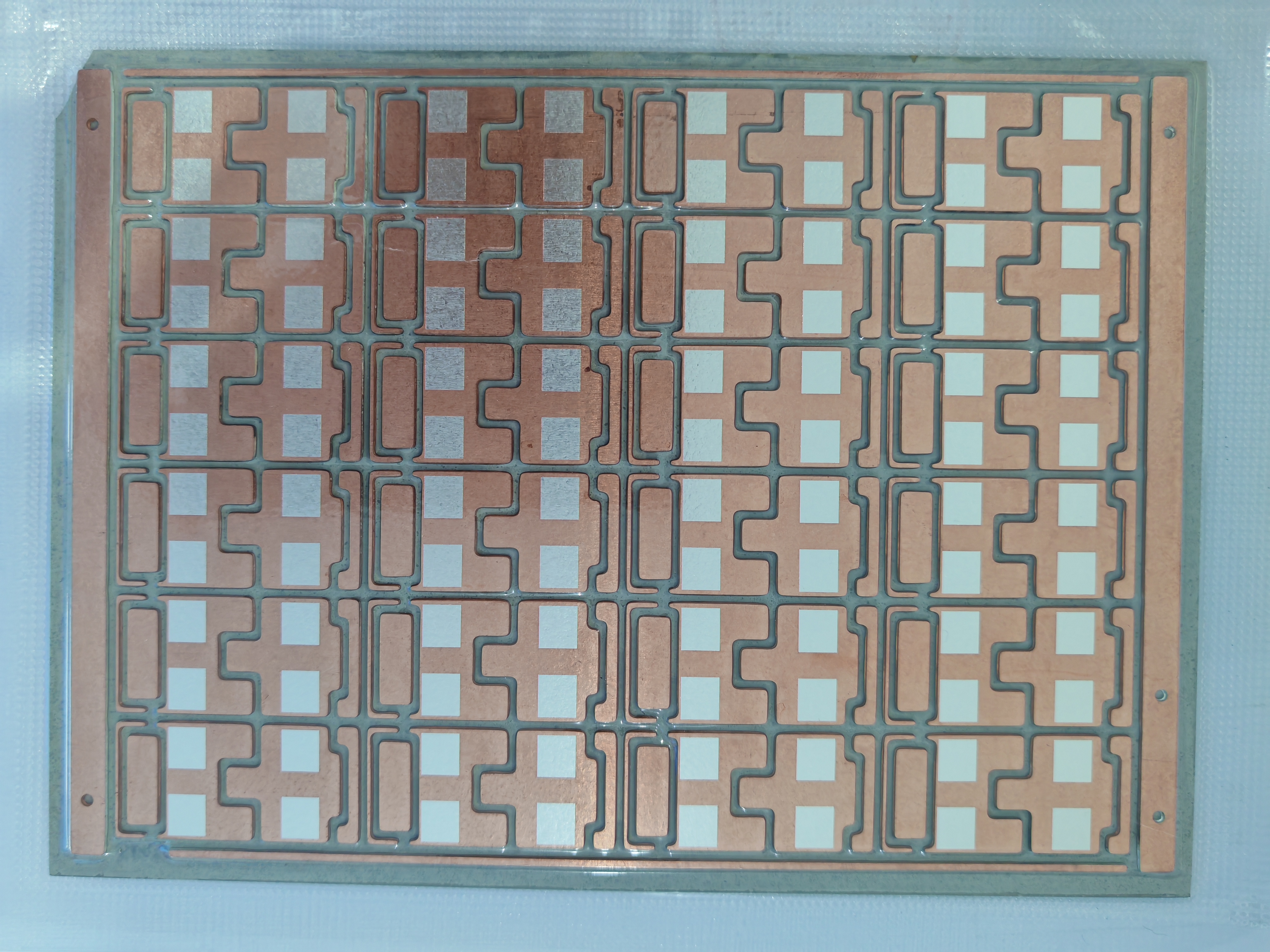
AMB Silicon Nitride Ceramic Copper-Clad Substrate
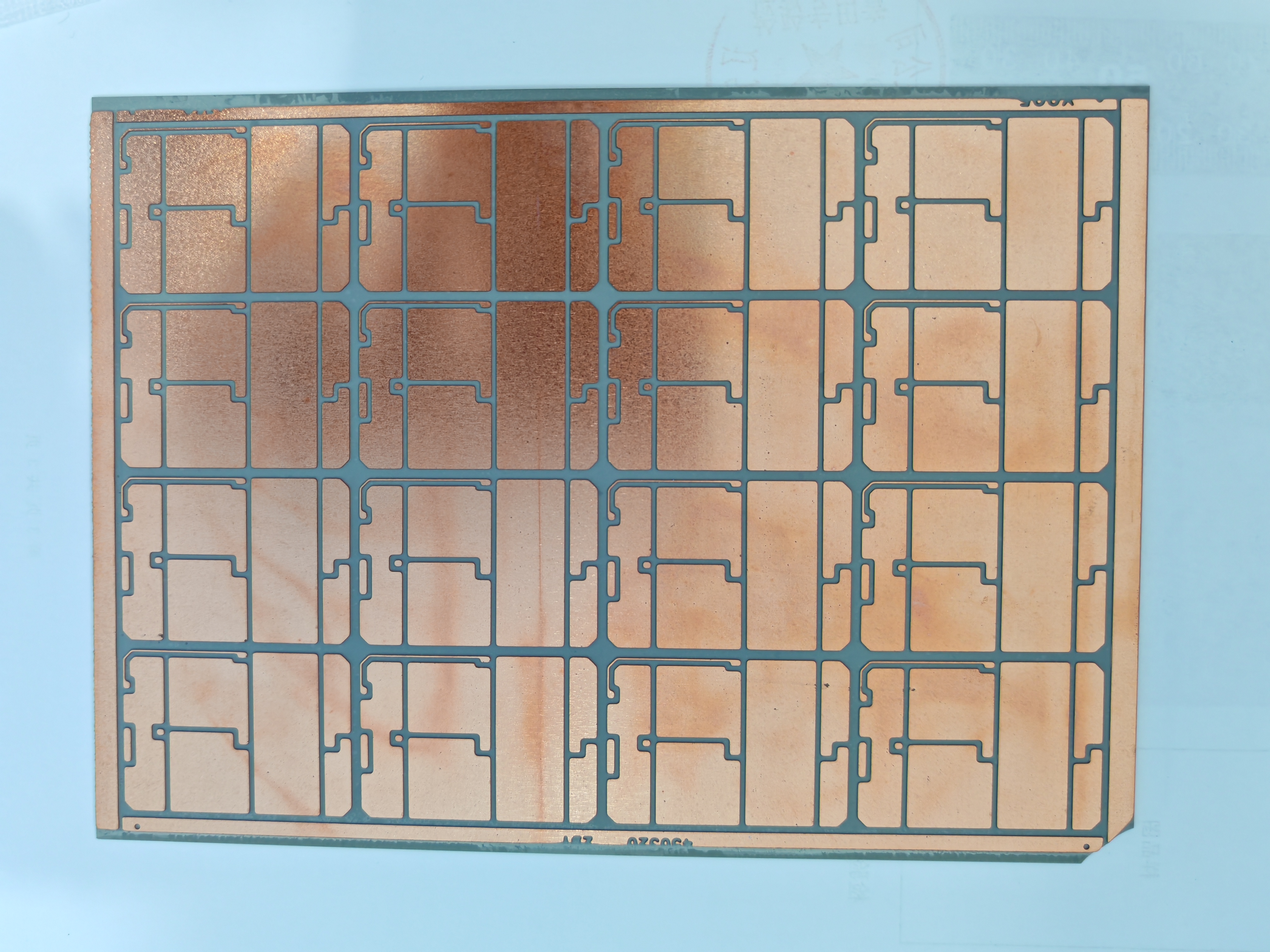
AMB Silicon Nitride Ceramic Copper-Clad Substrate
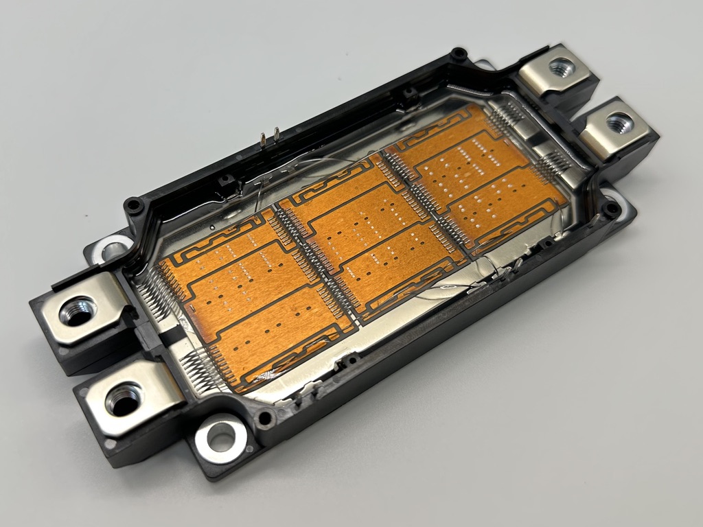
IGBT Module
 浙公网安备33041102000682号