Research
Our research is centered on advanced electronic packaging, thermal management materials, and intelligent functional devices, with an emphasis on the coordinated development of materials design, fabrication, characterization, and application.
Electronic Packaging
Research in this area focuses on highly thermally conductive and reliable electronic packaging materials and interconnection technologies, including conductive adhesives, thermal interface materials, and low-temperature transient liquid-phase micro/nano interconnects, aiming to enhance the thermal and electrical performance as well as long-term reliability of electronic devices.
Thermal Management Materials
This area explores advanced materials for efficient heat conduction, thermal insulation, and flame retardancy, with particular attention to multiscale structural optimization and applications in new energy vehicles, aerospace systems, and energy storage devices.
Functional Materials and Devices
Research in this area is devoted to the development of functional materials and devices with intelligent response characteristics, including thermal switching materials, electromagnetic absorption materials, and shielding materials, with broad applications in information technology, energy storage, and energy conversion.
Research Highlights
The group is distinguished by an integrated research approach that combines theoretical analysis, computational modeling, experimental validation, and engineering application. Strong emphasis is placed on interdisciplinary collaboration, with systematic efforts spanning microstructural design, property optimization, and device integration.
By establishing a complete research chain from materials design to application-oriented validation, the group is committed to advancing the practical deployment of high-performance materials in electronic information technologies, advanced manufacturing, new energy systems, and high-end equipment.
Facilities and Equipment
The laboratory is equipped with extensive resources for both bulk-scale and micro/nanoscale materials fabrication and characterization. Major instruments include a Raman spectrometer, frequency-domain thermoreflectance thermal conductivity measurement system, 1D/2D material transfer platform, thermal conductivity analyzer, interfacial thermal resistance and thermal conductivity measurement system, snap-action/twist-action cooling system, machine learning workstation, stereolithography 3D printer, fused deposition modeling 3D printer, hot press, vulcanizing press, ultrasonic crusher, planetary ball mill, atomic force microscope, and reactive ion etching system.
In addition, the analytical and testing center provides access to electron microscopy facilities, physicochemical measurement and characterization platforms, as well as cleanroom and micro/nanofabrication platforms. Available services include high-resolution transmission electron microscopy (HR-TEM), high-angle annular dark-field scanning transmission electron microscopy (HAADF-STEM), benchtop X-ray absorption fine structure/emission spectroscopy (XAFS/XES), scanning electron microscopy (SEM), X-ray diffraction (XRD), and X-ray photoelectron spectroscopy (XPS).
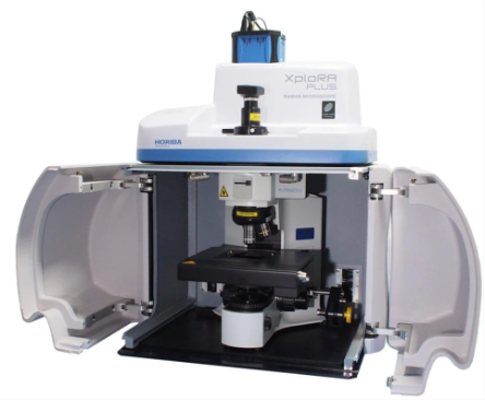
Raman Spectrometer
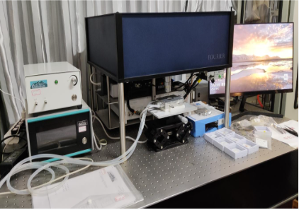
Frequency-Domain Thermoreflectance System
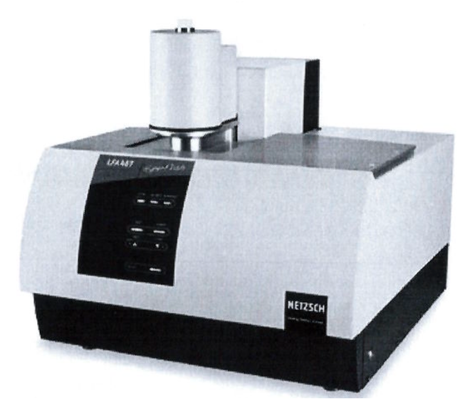
Thermal Conductivity Analyzer
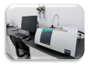
Thermogravimetric Analyzer
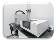
Differential Scanning Calorimeter
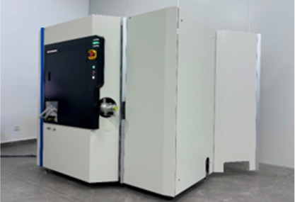
X-ray Photoelectron Spectrometer
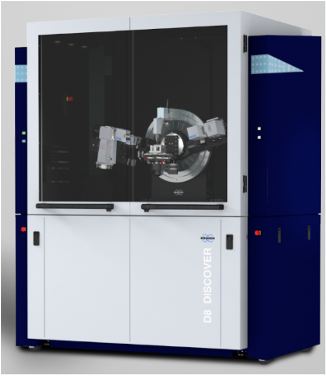
X-ray Diffractometer
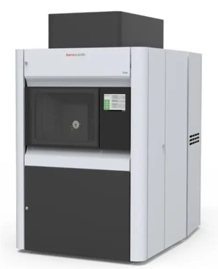
Transmission Electron Microscope
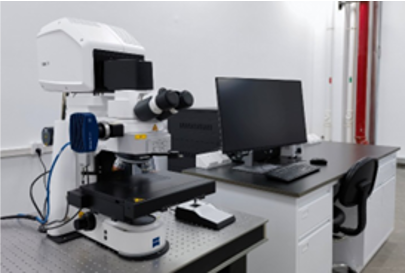
Laser Confocal Microscope
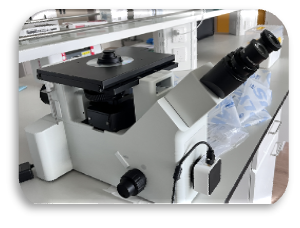
Multifunctional Inverted Microscope
Infrared Spectrometer
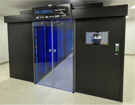
High-Performance Computing Cluster
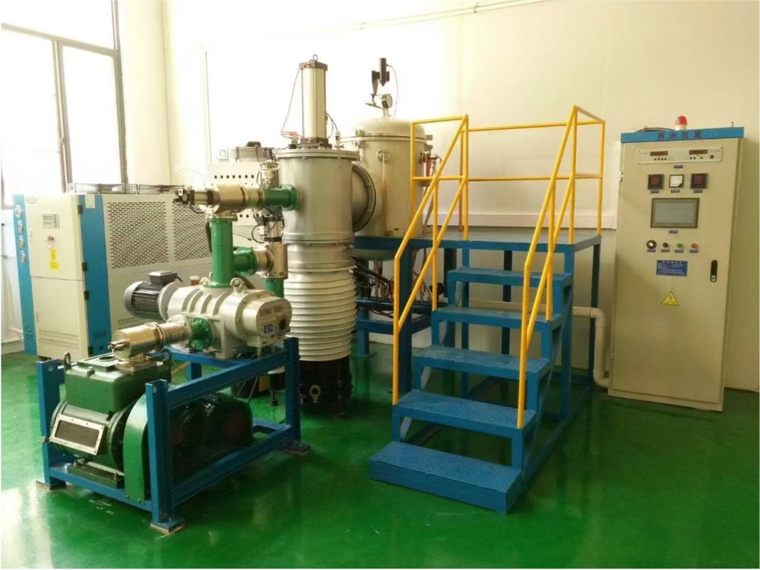
High-Thermal-Conductivity Vacuum Hot-Press Furnace
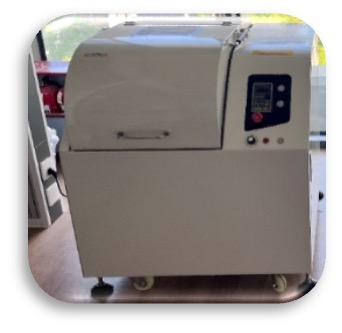
Planetary Ball Mill
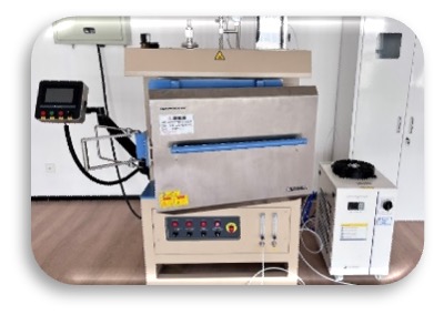
Vacuum Annealing Furnace
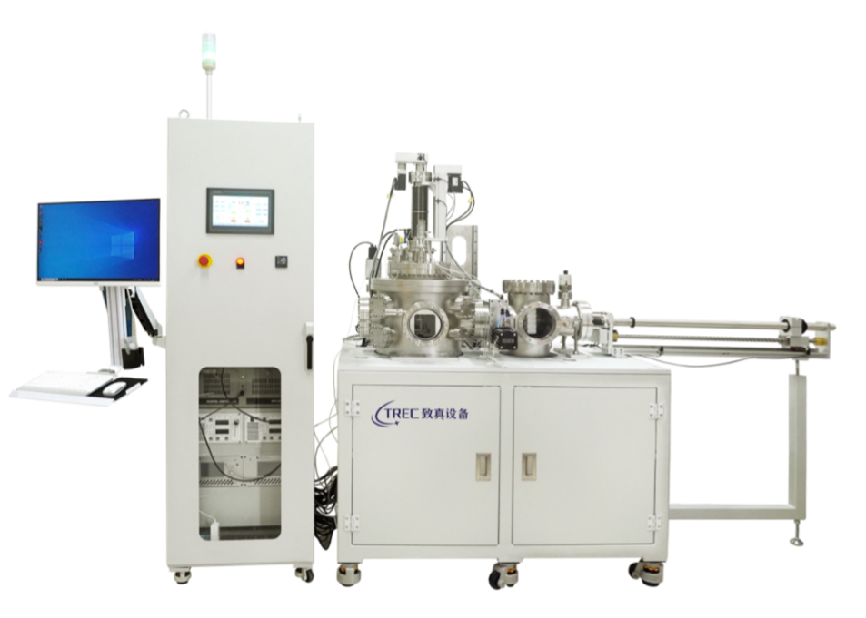
Ultra-High-Vacuum Additive Thin-Film Growth System
 浙公网安备33041102000682号